Equipment Capabilities
Explore the equipment available for your use at the TNFC and learn about their capabilities. TNFC facilities are open to both academic and industrial researchers, making the centre an ideal choice for open-access prototype development and testing. Key research areas include: Microelectronics, Photonics, Integrated Optics and Nanomaterial Processing. With two facilities to serve you, the TNFC is Canada's premier hub for semiconductor research and education.
TNFC capabilities include:

Electron Beam Lithography
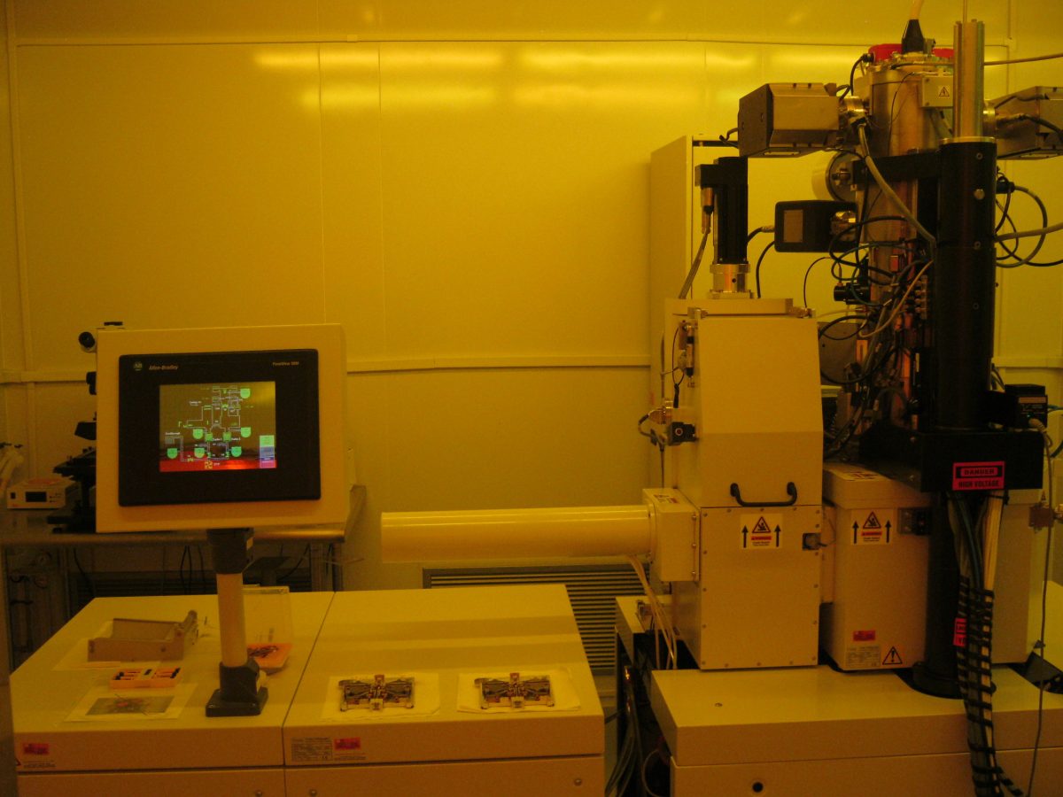
Raith EBPG 5000+ Electron Beam Lithography System
The EBPG 5000+ is a state-of-the-art Gaussian beam vector scanning electron beam lithography system.
- Acceleration Voltage: 100 kV
- Maximum Field Size: 1024 x 1024 µm2 (20 bit)
- Maximum pattern generator frequency: 50 MHz
- Beam current: 50 pA to 300 nA
- Substrate size: 1 to 15 cm
- Exposure Resolution: < 10 nm
- Field Stitching Accuracy: 20 nm (mean + 3σ)
- Overlay Accuracy: 20 nm (mean + 3σ)
- Positioning Accuracy: 0.6 nm (interferometric stage)
Pattern fracturing, and the associated options and capabilities, is the heart of Layout BEAMER package. The Layout BEAMER software interprets design data and converts it into the formats needed to write with the EBPG 5000+ system.
- Input File Format: All major formats (GDSII, CIF, DXF, LTXT, bitmap)
- Integrated Layout Editor
- Layout Operations (healing, biasing, tone reversal, merge, Boolean operations)
- Proximity Effect Corrections (PEC)
- Advanced fracturing (arbitrary shapes, curved fracturing, field position control)
- Output File Format: GPF
- Single user (one at a time), floating (network) license
Nanolithography Wetbenches
The Wallberg Nanolithography Facility hosts two VPFX-6 microzone wetbench stations dedicated to substrate cleaning, EBL resist spin coating, curing, development and removal.
- Provides a class 100 (ISO Class 5) working environment
- Segregated, dedicated wetbench stations and resist spinners for positive tone & negative tone resist preparation
- Vacuum enabled, dedicated hotplates with digital control
- Includes DI water, nitrogen gas utilities and all necessary chemical supplies for EBL resist preparation
Thin Film Thickness Measurement System
The Thin Film Thickness Measurement System provides a quick and reliable solution for measuring the thickness of translucent or low absorbing thin films from 10 nm to 50 um with 380 nm – 1000 nm spectral range. The measurement is based on specular reflectance and uses tungsten halogen light source (360-2400 nm), high-resolution spectrometer, 400 µm diameter fiber optic reflection probe, and a manual stage. User-friendly software (TFCompanion) complements the setup.
ShelLab 1330GM Gravity Convection Oven
The ShelLab 1330GM Gravity Convection Oven is hosted by the Wallberg Nanolithography Facility and is used primarily for post-bake of electron beam lithography resists on sample substrates.
- Recovery Time: 10 minutes at 150°C
- Heat-up Time: 15 minutes to 150°C
- Temperature Uniformity: ± 2.0°C at 150°C
- Temperature Range: 40ºC to 240ºC
- Digital electronic timer
Nikon Eclipse LV100 Microscope
Nikon’s Eclipse LV100 microscope, available in diascopic and episcopic microscope illumination modes, produces bright, clear, and high contrast images. The microscope has 4 objectives (x5, x10, x20, x50, x100), a 6 x 4” stage and a DS-Fi1 camera. Image processing is possible with the Nikon NIS-elements D3.0 imaging software.
Lithography User Recipes
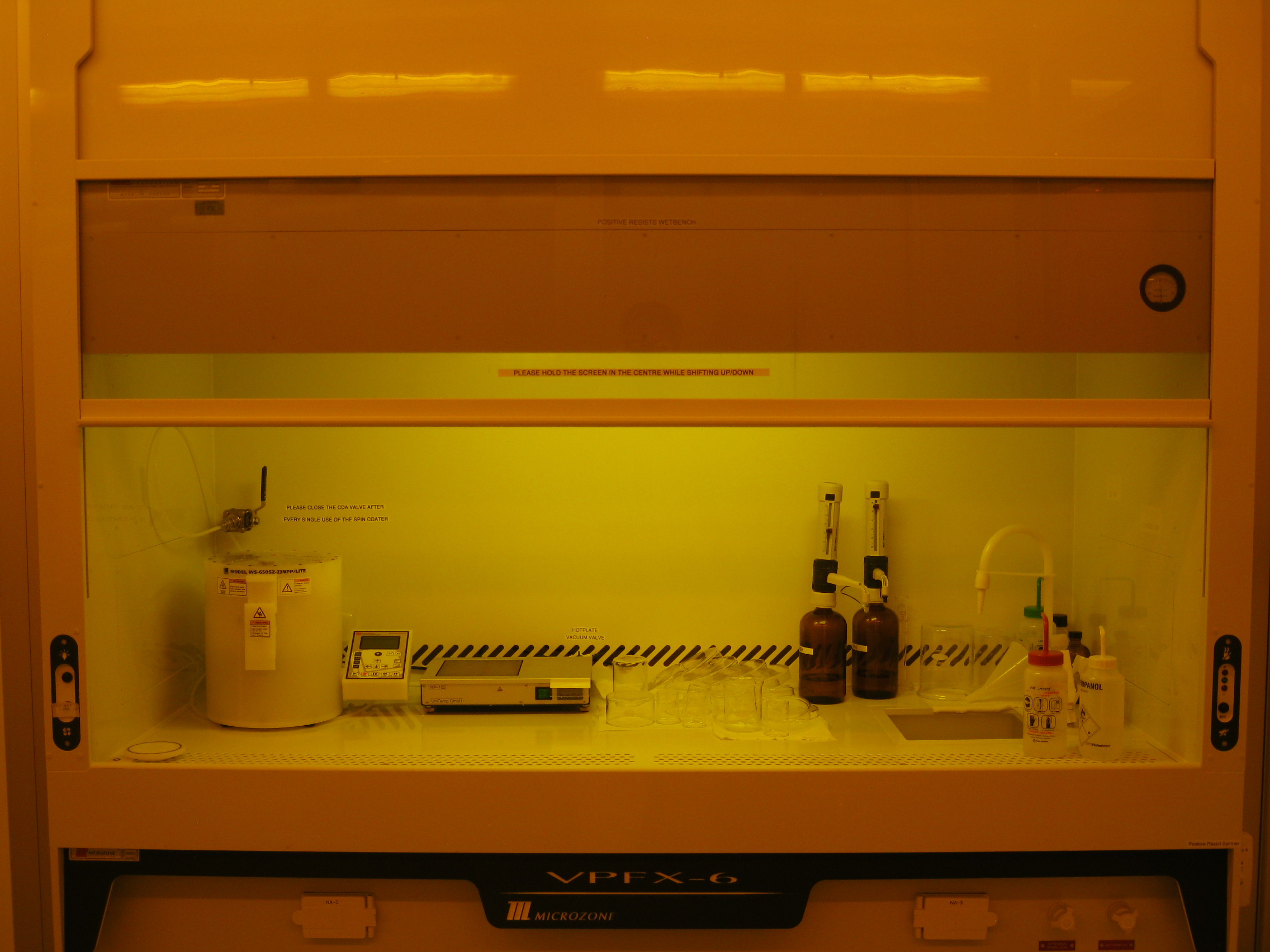
Download PMMA Resist PDF here.
Download Copolymer Resist PDF here.
Download Double Layer Resist PDF here.
Download ZEP520A Resist PDF here.
Download AR-P-6200 Resist PDF here.
Download ma-N 2400 Resist PDF here.
Download XR-1541 Resist PDF here.
Download TNFC Quick Guide APOGEE Bake Plate formatted PDF here.
Photolithography
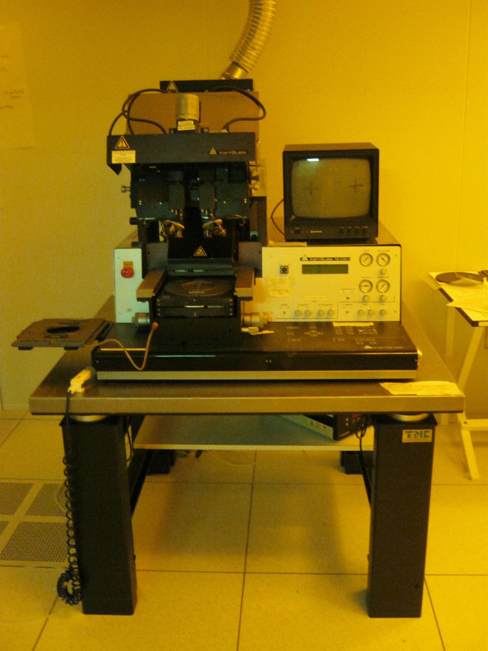
Suss MicroTec MA6/MA4 Mask Aligners
The MA6 and MA4 Mask Aligners use UV light to transfer patterns from photomasks onto substrates coated with photoresist.
- Exposure Resolution: < 1 µm
- Alignment accuracy: Topside – 500nm
- Exposure modes: Hard contact, soft contact, proximity, flood
- Spectral range: 365nm – 405nm
- Substrate accommodation: 1cm2 pieces and wafers up to 4″(MA4) or 6″ (MA6)
- Uniformity: +- 5% over exposure area
- CCD camera and monitor for image capture
Photolithography Wetbench
The Pratt Microfabrication Facility hosts a photolithography wet processing station dedicated to substrate cleaning, photoresist spin coating, curing, development and removal.
- Provides a class 10 (ISO Class 4) working environment
- Segregated wetbench stations and resist spinners for positive tone & negative tone resist preparation
- Multiple hotplates available with manual control
- Includes DI water, nitrogen gas utilities and all necessary chemical supplies for photoresist preparation
Deposition
Oxford Instruments PlasmaLab System 100 PECVD
The PlasmaLab System 100 PECVD system is hosted by the Pratt Microfabrication Facility, and is configured to deposit high quality silicon dioxide, silicon nitride and silicon oxynitride films with thicknesses up to several microns via a plasma-assisted chemical reaction process.
- Available Chemistries: 5% SiH4 in 95% N2, NH3, N2O, N2, Ar, He and 80% CF4 in 20% O2
- Substrate accommodation: Small samples up to 8″ wafers
- Deposition temperature: 250C – 400C
- Typical Rate: 4-40 nm/min (oxide), 10-100 nm/min (nitride)
- Automated sample loading with load-lock chamber
Expertech CTR-200 LPCVD
The Expertech CTR-200 LPCVD system is hosted by the Pratt Microfabrication Facility, and is configured to deposit high quality silicon nitride films via a high temperature, low-pressure chemical reaction process.
- Available Chemistries: 1:3 H2SiCl2:NH3 (Stoichiometric), 4:1 H2SiCl2:NH3 (Low-Stress)
- Substrate accommodation: 4″ and 6″ wafers
- Deposition Temperature: 760C – 880C
- Typical Rate: 3-4 nm/min
Bruce Technologies Oxidation Furnace
The Bruce Oxidation Furnace is hosted by the Pratt Microfabrication Facility. The furnace is able to grow oxide films on silicon wafers using a dry or wet oxidation process.
- Substrate accommodation: Up to 4” wafers (batches)
- Temperature recipes available up to 1250C
- Wet & dry oxidation chemistries available
- Programmable multi-step temperature ramping
- Motorized loading arm for wafer boats
AJA International ATC Orion 5 Sputter Deposition System
The ATC Orion 5 Sputter Deposition System is hosted by the Pratt Microfabrication Facility. The system is used to deposit thin film dielectric and metal materials (including magnetic materials) onto wafer substrates via a plasma-induced sputter deposition process.
- Targets: See Process Database for Materials
- Argon, oxygen, and nitrogen plasma capability
- Substrate accommodation: Small pieces up to 6″ wafers
- Wafer heating via quartz halogen lamp (RT – 850C)
- Software controlled multi-step recipe design
- Substrate RF/DC biasing capability
- Typical Rate: 0.5-3 Å/s
Angstrom Nexdep Electron Beam Evaporator
The Angstom Nexdep Electron Beam Evaporator is hosted by the Pratt Microfabrication Facility. The system is used to deposit thin metal films onto wafer substrates using an electron-beam vapor deposition process.
- Source Materials: Au, Al, Cr
Deposition User Recipes
PECVD Recipes
Oxide & Nitride Deposition Recipes
Material | Temperature (ºC) | Pressure (mTorr) | Gas flow (sccm) | Power (W) | Deposition rate (nm/min) |
SiO2 | 300 | 400 | 30 5%SiH4/N2, 700 N2O | 45 | 4 |
SiO2 | 300 | 1000 | 170 5%SiH4/N2, 710 N2O | 30 | 40 |
Si3N4 | 300 | 650 | 400 5%SiH4/N2, 20 NH3, 600 N2 | 40 (LF, Pulse: 7), 50 (RF, Pulse: 13) | 10 |
Si3N4 | 300 | 1800 | 450 5%SiH2/N2, 10 NH3, 1000 N2, 1000 N2O | 160 (LF, Pulse: 10), 200 (RF, Pulse: 10) | 100 |
Clean | 300 | 1300 | 150 80%CF4/O2 | 200 | – |
LPCVD Deposition Recipes
Nitride Deposition Recipes
Process | Temp. (ºC) | Pressure (mTorr) | Gas flow (sccm) | Deposition rate (nm/min) |
Stoichiometric | 770 | 200 | NH3:DCS 24:100 | 2.68 |
Low Stress | 800 | 200 | NH3:DCS 100:25 | 4.40 |
Sputter Deposition Recipes
Metal Sputtering (DC Power)
Material | Default Gun # | Pressure (mTorr) | Gas flow (sccm) | DC Power (W) | Sputter rate (Å/s) |
Ni | 1 | 3 | 30 Ar | 200 | 1.8 |
Cu | 1 | 3 | 30 Ar | 200 | 3.1 |
Ti | 2 | 3 | 30 Ar | 200 | 0.8 |
Al | 2 | 3 | 30 Ar | 200 | 1.1 |
Cr | 2 | 3 | 30 Ar | 200 | 1.5 |
W | 5 | 3 | 30 Ar | 200 | 0.8 |
Ta | 5 | 3 | 30 Ar | 200 | 1.4 |
Dielectric Sputtering (RF Power)
Material | Default Gun # | Pressure (mTorr) | Gas flow (sccm) | RF Power (W) | Sputter rate (Å/s) |
Si | 3 | 3 | 30 Ar | 300 | 1.0 |
SiO2 | 3 | 3 | 30 Ar | 300 | 0.7 |
Si3N4 | 3 | 3 | 30 Ar | 150* | 0.22 |
Al2O3 | 4 | 3 | 30 Ar | 250* | 0.16 |
MgO | 4 | 3 | 30 Ar | 300 | 0.1 |
ITO | 4 | 3 | 30 Ar | 50* | 0.3 |
*Maximum power permitted based on published maximum power density.
Parylene Coating Recipes
Parylene Type-C Recipes
Parylene Source (g) | Film Thickness (nm) |
0.15 | 100 |
2.2 | 1000 |
15 | 7000 |
Etching
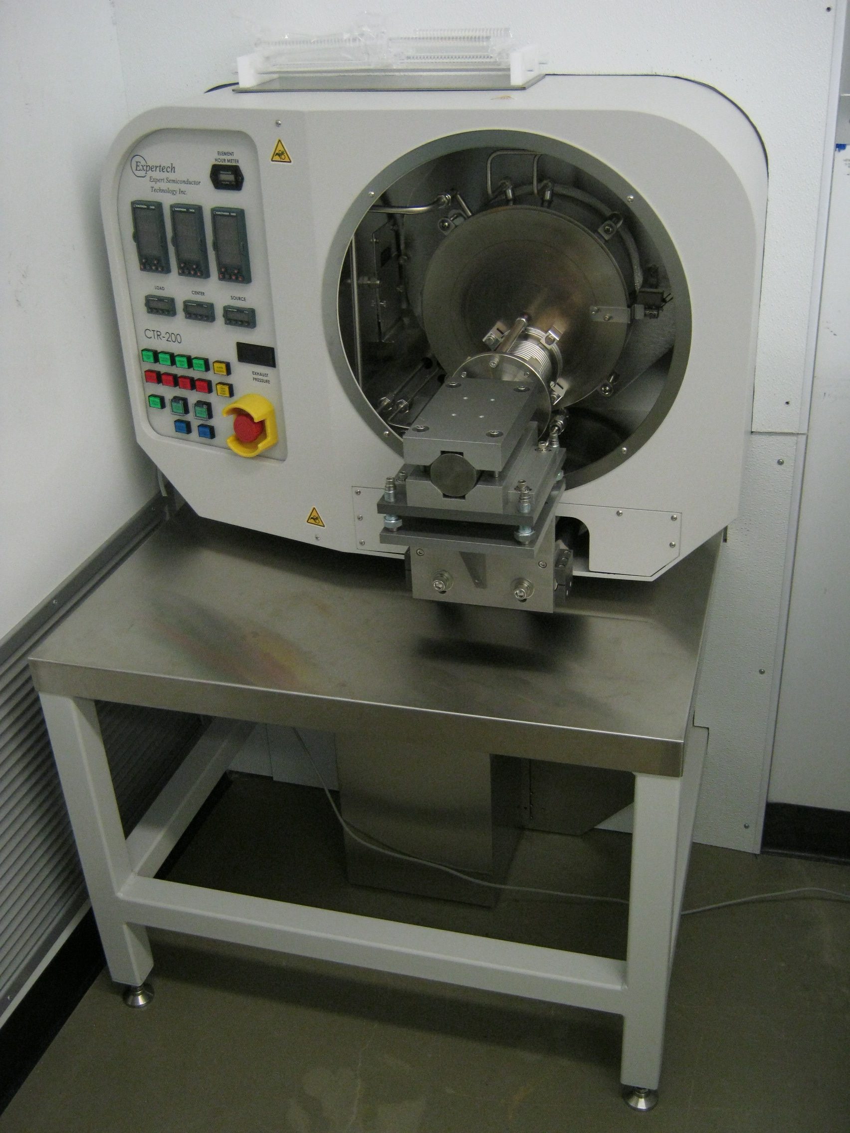
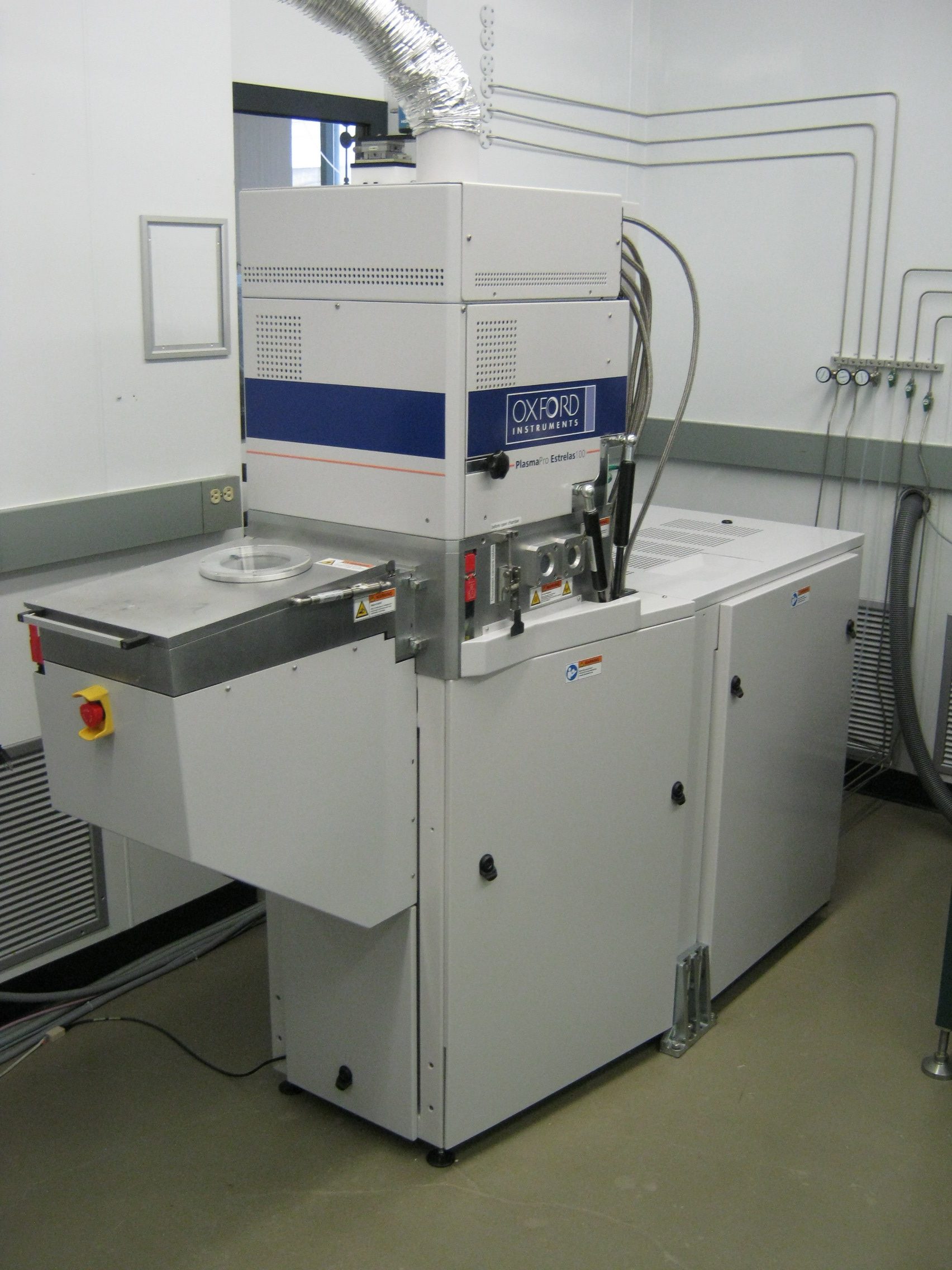
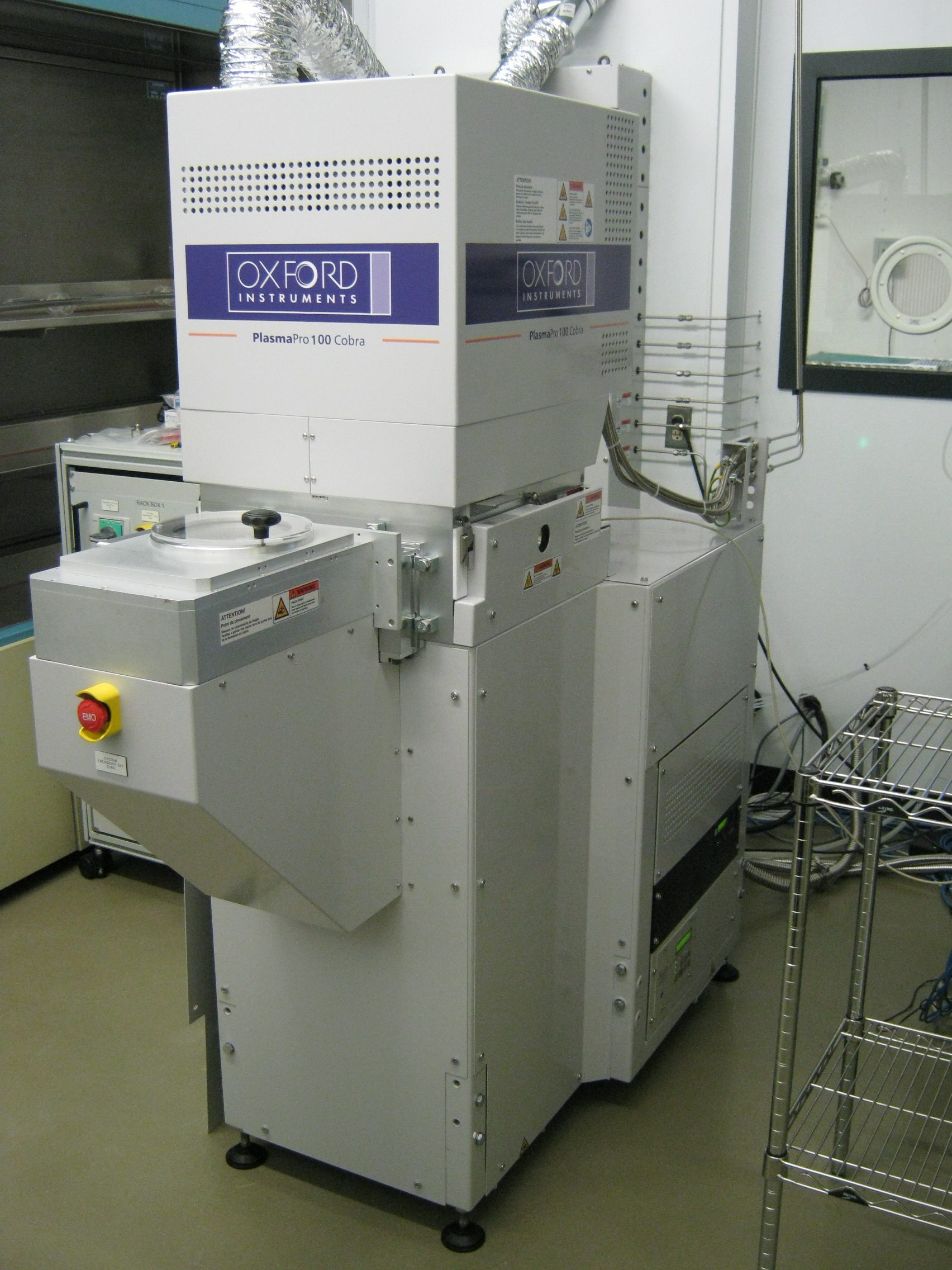
Oxford Instruments PlasmaPro Estrelas100 DRIE System (Si)
The PlasmaPro Estrelas100 DRIE System is hosted by the Pratt Microfabrication Facility. The system is used to etch high aspect-ratio anisotropic etch cavities into silicon-based substrates.
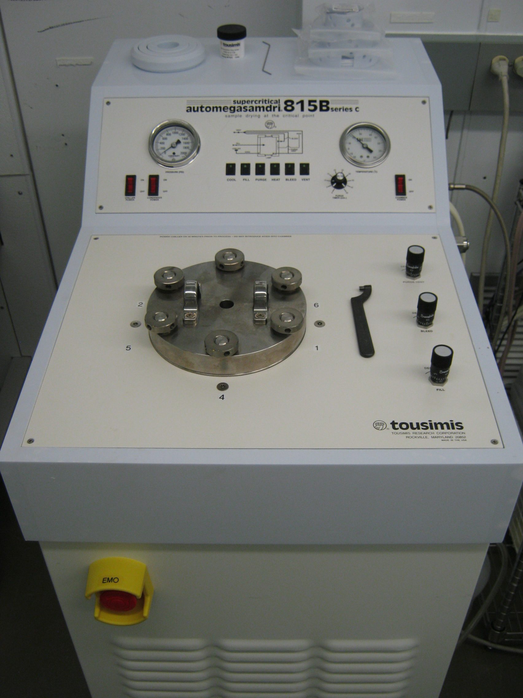
- Compatibility with Si and SiO2 substrates
- Substrate accommodation: Small pieces up to 6″ wafers
- Etch Rate: > 25 µm/min (Bosch), > 5 µm/min (Cryo), > 0.5 µm/min (Mixed)
- Uniformity: < ± 3% (Bosch), < ± 5% (Cryo), < ± 5% (Mixed)
- Maximum aspect ratio: 70:1 (Bosch), 30:1 (Cryo), 7:1 (Mixed)
- Selectivity to PR: > 250:1 (Bosch), > 100:1 (Cryo), > 10:1 (Mixed)
- High plasma stability, eliminating ‘first wafer effect’
Oxford PlasmaPro 100 Cobra ICP-RIE (Si)
The Oxford PlasmaPro 100 Cobra ICP-RIE System is hosted by the Pratt Microfabrication Facility. This tool is used to perform inductively-coupled plasma (ICP) reactive ion etching on silicon based materials, including SiO2, Si3N4, and isotropic etching on Si.
- Etch Chemistries: SF6, CHF3, CF4, O2
- SiO2, SiN, and isotropic Si etching
- Substrate accommodation:
- ICP to improve etch rates, profile control, uniformity and selectivity
- Easy-to use computer interface
TePla Technics 100-E Oxygen Plasma Asher
The Technics 100-E is a Plasma Asher is available for resist stripping and descum processes. The system is hosted by the Wallberg Nanofabrication Facility
- Maximum substrate size: 100 mm2 sample or 4″ wafer
- Plasma chemistry: Oxygen only
- Ultimate Pressure: < 8 x 10⁻⁵ Torr
Etching Wetbenches
The Pratt Microfabrication Facility hosts two wet processing stations configured for wet etch processes.
- Controlled laminar flow provides a safe class 10 (ISO Class 4) working environment
- Chemistries supported: HF etch, piranha etch, KOH etch, H3PO4 etch, buffered-oxide etch, chrome etch
- Includes all necessary glass and plastic containers for small samples up to 8″ wafers.
- Includes DI water, nitrogen gas utilities, protective sashes, controlled exhaust, acid-resistant gloves, face shields and aprons.
Dicing & Packaging
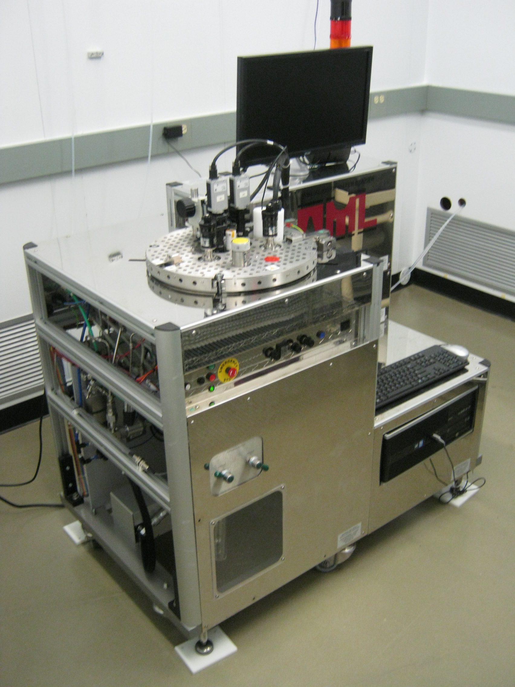
AML AWB-04 Aligner Wafer Bonder
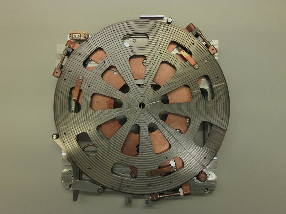
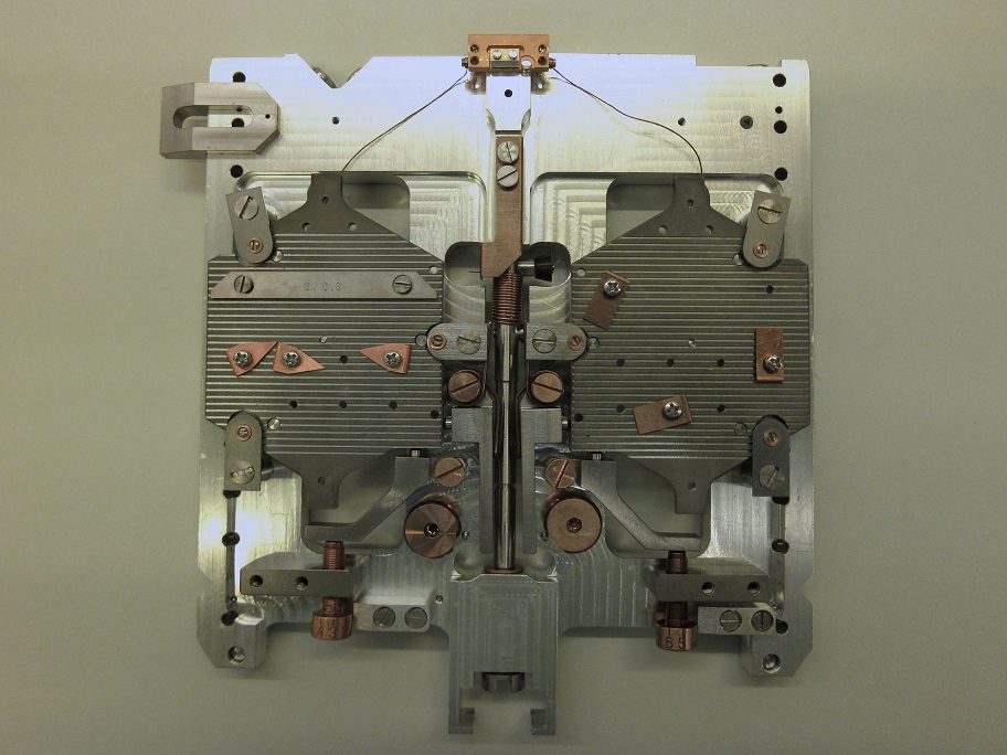
The AWB-04 Aligner Wafer Bonder is hosted by the Pratt Microfabrication Facility. This tool is used to seal and encapsulate MEMS/IC device structures and create 3D interconnects on wafer-level devices.
- Anodic, Direct (Radical Activated), Eutectic, Glass Frit, UV Adhesive, Solder & Thermocompression Bonding
- In-situ alignment accuracy: 1 micron
- 10-6mbar Vacuum to 2bar process gas
- Substrate accommodation: Small chips and 3″- 4″ wafers
- Temperature Range: Up to 560° C
- In-situ UV cure capability
- Configured to support aligned polymer micro hot embossing and nano-imprinting
SCS 2010 Parylene Coater
The SCS 2010 Parylene Coater is hosted by the Pratt Microfabrication Facility. The tool is capable of depositing parylene films onto device chips and wafers, protecting them against moisture, dust, chemicals, and temperature extremes that may otherwise cause damage.
- Parylene-C coating only
- Closed-loop parylene vapor-pressure control
- Sample sizes up to 15 cm x 15 cm
- Parylene dimer capacity up to 100 gm
- Three-layer rotating fixture
Disco DAD3220 Automatic Dicing Saw
The DAD3220 Automatic Dicing Saw is hosted by the Pratt Microfabrication Facility. This tool is used to perform high precision dicing of silicon wafers or glass substrates into smaller chips.
- Auto-alignment, auto-focus, and auto-kerf check functions
- Unlimited configurable independent user programs
- 4 programmable cutting channels with 320 degree max rotating angle
- Cutting blades thickness: 100 – 400 micron
- Max substrate size: 6” wafers or 6″ x 6″ substrates
- 160mm x 162mm cutting range
- < 0.005/160 positioning accuracy
- 1.5 kW spindle at 30,000 per minute
Tousimis Autosamdri-815B Supercritical Point Dryer
The Autosamdri-815B Supercritical Point Dryer is hosted by the Pratt Microfabrication Facility. This tool is used to remove liquid from processed MEMS/NEMS devices without subjecting delicate structures to potentially destructive surface tension forces that are generated during the liquid-to-gas phase change.
- 4″, 3″, 2″ diameter wafer holders and 10mm square die holders included
- Holders are HF compatible and can hold up to 5 wafers or die per process
- Unique chamber inserts maximize efficiency in LCO2 consumption and process time
- Internal filtration system delivers clean LCO2 into process chamber down to 0.4µm
- Chamber illumination with viewing window
- Automatic processing with status LEDs
TPT HB16 Wire Bonder
The HB16 Wire Bonder is hosted by the Pratt Microfabrication Facility. This tool is used to bond thin, electrically conductive metal wire or ribbon between precise locations on chips, slides, printed circuit boards, etc. This technique can be used to complete electrical pathways to small chips for subsequent device characterization or use with larger circuit elements.
- Bond metals: Au, Al in wire and ribbon.
- Ball-wedge and wedge-wedge bonding
- A comprehensive loop profile library
- Automatic, semi-automatic and step modes
- 100 customizable user programs
- Pull testing equipment (bond strength measurement)
- Stitch bonding capability
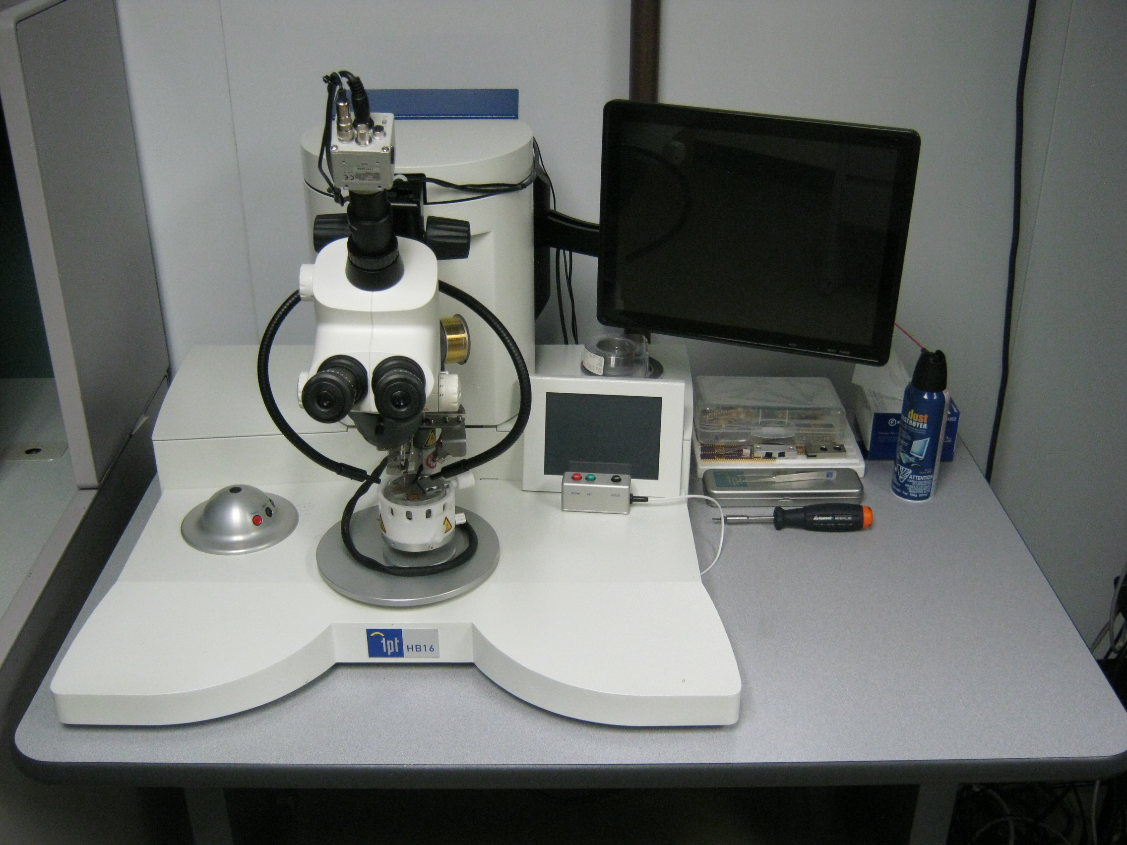
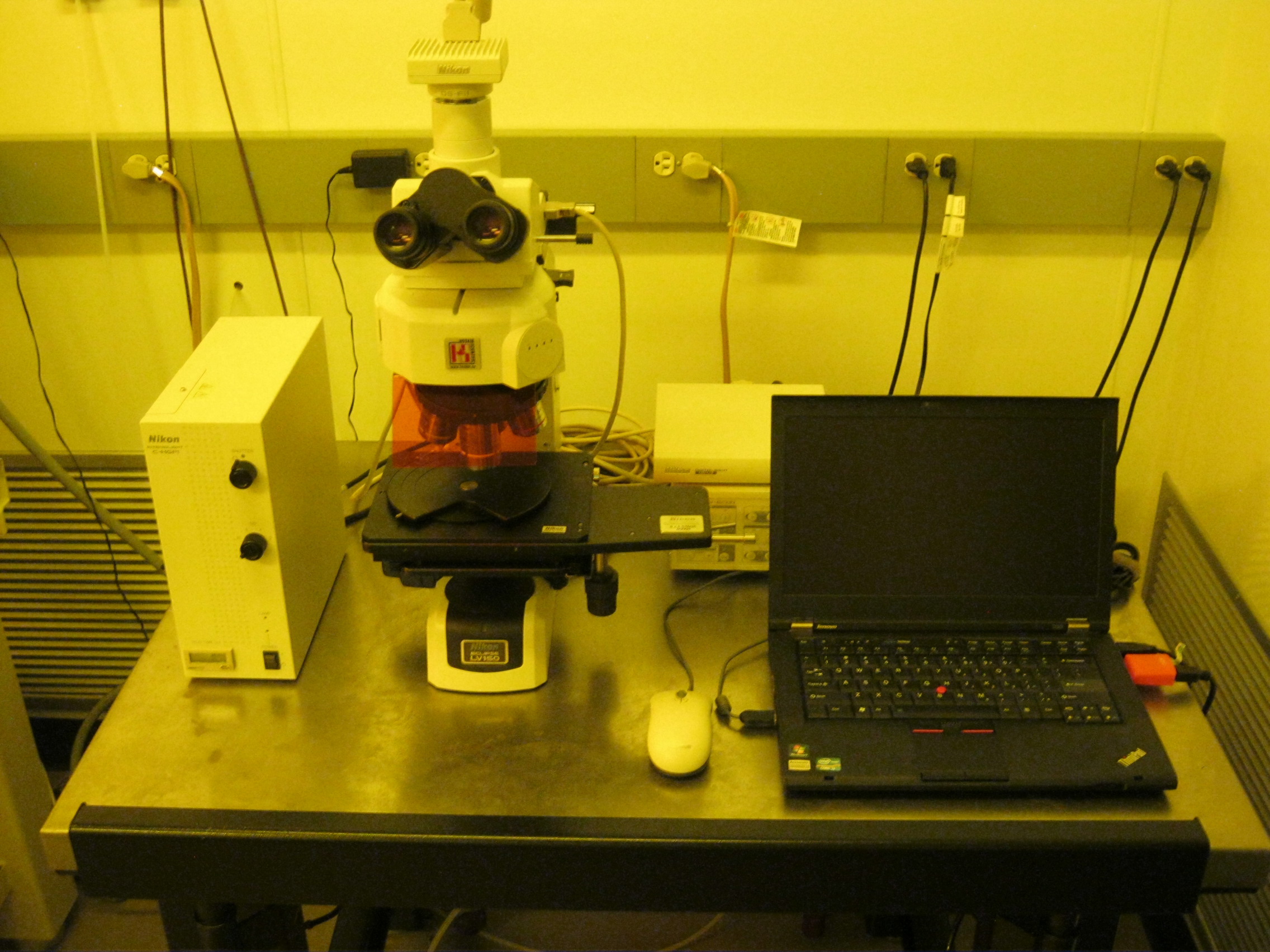
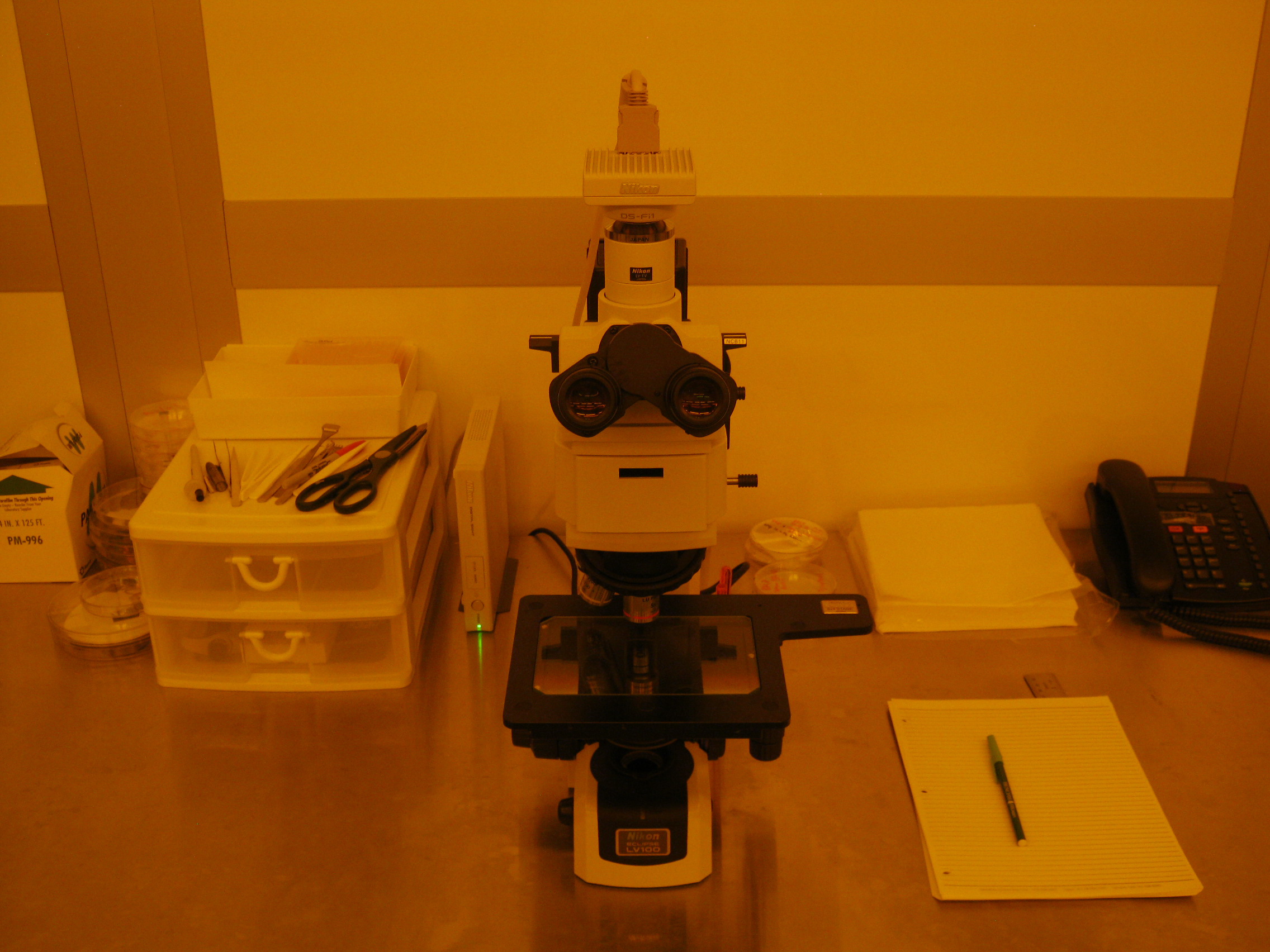
Imaging & Characterization
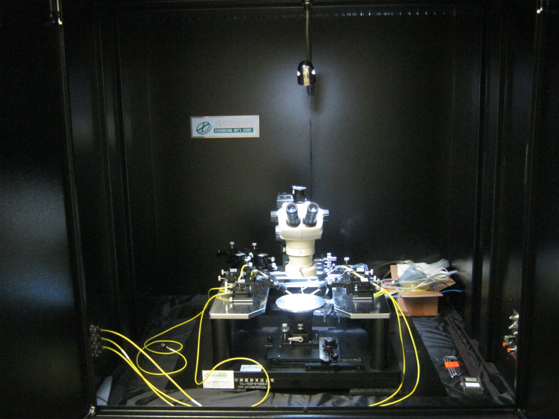
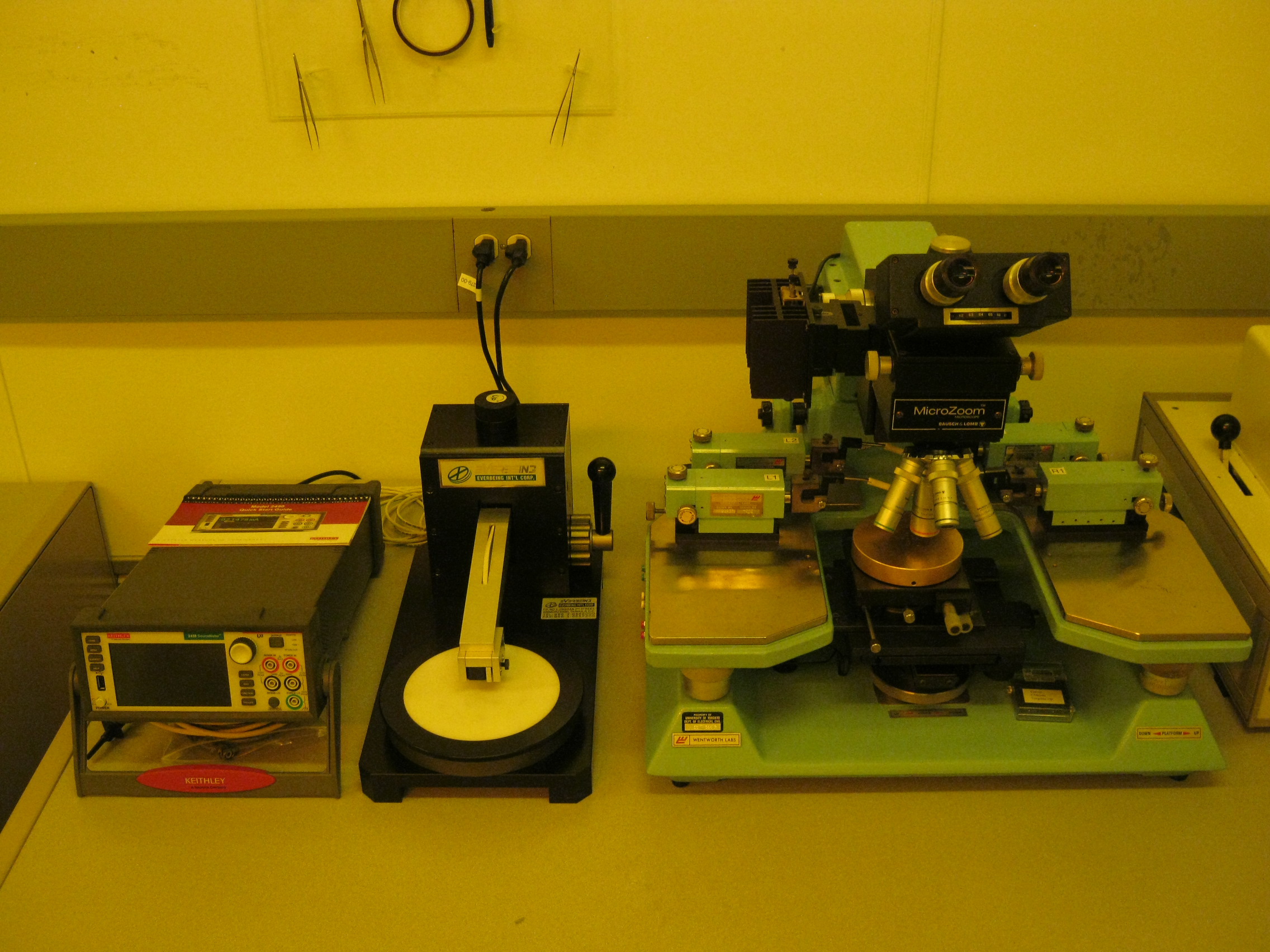
Probe Stations
Two probe stations are hosted by the Pratt Microfabrication Facility, including one probe station generously donated by Everbeing Int’l Corp.
Keithley SMU 2400 Graphical Series Sourcemeter
The SMU 2400 Sourcemeter is hosted in the Pratt Microfabrication Facility, and was generously donated by Tektronix, Inc.
HP 4155A Semiconductor Parameter Analyzer
The 4155A Semiconductor Parameter Analyzer is hosted by the Pratt Microfabrication Facility.
Nikon 3D Microscope
The Nikon 3D Microscope is hosted by the Pratt Microfabrication Facility.
Optical Microscopes
TNFC facilities provide access to optical microscopes for visual analysis of devices and samples.
Horiba Joben Yvon UVISEL Ellipsometer
The UVISEL Ellipsometer is hosted by the Pratt Microfabrication Facility.
Dektak Profilometer
Device Processing User Recipes
Wire Bonding Recipes
Bond Parameters
Parameter | Bond 1 | Bond 2 |
Ultrasonic (US) | 350 | 350 |
Time (ms) | 400 | 400 |
Force (mN) | 450 | 450 |
Heat (ºC) | 120 | 120 |
Default ball bond parameters for 1 mil (25 μm) gold wire are outlined above. Adjustment (i.e. ±25, ±50) may be required to achieve successful bonds.
NOTE: Successful bond parameters may vary significantly depending on wire/pad materials, surface contamination/oxidation, thermal contact with heated stage, etc.